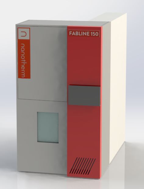

NANOTHERM FABLINE
an ekrubnano company
 |
150 mm- 200 mm VERTICAL FURNACE PROCESSING
THERMAL PROCESSING TECHNOLOGY
Detailed Parameters of the Product
Overview Vertical furnace with small footprint for high-quality processing.
Applications
The Nanotherm Fabline can process 150mm - 200mm wafers up to 50 at a time. Carefully selected hardware and control system features enable continuous high temperature wafer processing. The Nanotherm Fabline vertical Furnace's also has the option to be capable of 1300C operation. The Nanotherm’s Primary Heating and Controls are manufactured by a proprietary source that has been producing high temperature furnaces heating systems up to 1300 °C since 1982
|
vertical furnac
Support

Specifications
|
Operational Temperature range |
Up to 1300 c deg |
|
Supported wafer sizes |
75mm to 200mm |
|
Maximum lot size |
12 wafer boat standard (50 wafers optional ) |
|
Gases used |
N2, Ar & N2 ,(other gasses available upon request) |
|
Applications |
Annealing Thermal oxide LPCVD Wet oxidation Dry oxidation SiC power devices |
|
Element Section Dimensions |
Configurable |
Die Deprocessing
Die delayering or deprocessing is that the
semiconductor failure analysis technique of denudation off the higher
layers of the die to show a defect web site that's buried beneath these
layers. Die delayering is sometimes done as a sequence of steps,
removing a layer or 2 at a time. Since every layer is with chemicals and
physically completely different from the others, the delayering steps are
completely different from one another further.
Descum
Photoresist residue sometimes remains after development, processing, and resist strip. Plasma treatment provides uniform removal of small quantities of resist over the entire surface of the wafer prior to further post processing.
Examples of other process application
l SEM/TEM sample cleaning for hydrocarbon contamination removal
Surface treat before biomedical coating and improve hydrophilicity of medical implants
Optics, glass and substrate cleaning before epoxy bonding
Photoresist ashing, descum and silicon wafer cleaning
PDMS, microfluidics, glass slides and lab-on-a-chip
Improve bonding for metal to metal or composite
Improve bonding for plastic, polymer and composite materials
Medical device activation, sterilization and improve coating adhesion
Cleaning before wire bonding, die attach, flip chip bonding process.

ekrubNano
EkrubNano is a U.S.-based manufacturer of plasma etch, equipment for specialty semiconductor and failure analysis, R & D and nanotechnology markets.
The EkrubNano team members are a collection of individuals with over 20 years in the plasma and semiconductor space and all have been innovators in plasma-processing equipment technologies.
Recent EkrubNano innovations include the new line of small desktop plasma RIE products to satisfy the FA and R&D markets. This market has been struggling with outdated equipment due the lack of and new logical choices.
EkrubNano’s advanced plasma-processing in research, pilot manufacturing, and volume production. EkrubNano is committed to the development of systems and services that meet the diverse requirements of our global customer base. The success of this commitment which EkrubNano strives to achieve with all endeavors. EkrubNano’s reputation as an industry leader is supported by more than 40 years of focus on customer support, product innovation, reliability, and low cost of ownership. The success of
EkrubNano systems in variety of manufacturing environments and research institutions has secured the company's status as a front runner supplier of plasma-process equipment.
CONTACT US
Phone:
408.614.0884
Email:
SALES@EKRUBNANO.COM
Office Hours: Weekdays 8:00 AM - 5;00 PM PST
Address:
Ekrub Nano
Pleasanton Ca 94566 USA

